
Introduction
Backilluminated CCD's are thin devices
(typically 10-20 microns thick) which become semitransparent in
the near infrared. Reflections between the nearly parallel front
and back surfaces of these devices cause them to act as etalons..
This etalon-like behavior leads to unwanted fringes of constructive
and destructive interference which artificially modulate a spectrum.
The extent of modulation can be very significant (over 20%) and
the spectral spacing of fringes, typically 5 nm, is close enough
to make them troublesome for almost all NIR spectroscopy.
A Review of Etalons
An etalon is a thin flat transparent
optical element with both surfaces highly reflective. This forms
a resonant optical cavity and only wavelengths which fit an exact
integer number of times between the surfaces can be sustained
in it. Because of this property, etalons can be used as comb filters,
passing just a series of uniformly spaced wavelengths. In an imperfect
etalon, the reflectance of the surfaces becomes less than 100%
and the spectral characteristics soften from a spiky comb to a
smooth set of fringes.
How Etaloning Works in a Backilluminated
CCD
 At
NIR wavelengths, the silicon that CCD's are made of becomes increasingly
transparent The back surface, where light enters a CCD in the
backilluminated configuration is typically antireflection coated.
These coatings are not perfect and their effectiveness varies
by wavelength. four).
At
NIR wavelengths, the silicon that CCD's are made of becomes increasingly
transparent The back surface, where light enters a CCD in the
backilluminated configuration is typically antireflection coated.
These coatings are not perfect and their effectiveness varies
by wavelength. four).
At wavelengths where silicon is transparent enough that light
can traverse the thickness of the CCD several times, one can expect
light to bounce back and forth between the two surfaces. This
increases the effective path length in the silicon and thus the
QE, but it also sets up a standing wave pattern. At long wavelengths,
several passes cause significant constructive or destructive interference.
A backilluminated CCD is typically about 17 microns thick. Since
the index of refraction of silicon is almost four, the effective
optical thickness is about 60 microns. The round trip optical
path length between the surfaces is thus about 120 microns. At
750 nm, this is 160 wavelengths. Thus there will be constructive
interference at 750 nm. The next wavelength where there will be
constructive interference will be where 161 wavelengths fit in
120 microns, about at 745 nm. Thus a pattern of constructive and
destructive interference will repeat at intervals of about 5 nm.
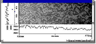
In a thin CCD, there are two types of etalon pattern, one spatial
and the other spectral a is not evident. In a backilluminated
the fringes are due to the variation of the wavelength, not the
thickness.
How to Avoid Etaloning
To tackle this problem, Princeton
Instruments has develop a backilluminated CCD which has maximum
etalon reduction. It combines three features:
1. The CCD is made on thick silicon, 40-50 microns. Since this is more than double the thickness of a normal backilluminated CCD, it significantly contributes to the absorption of NIR light, reducing the amount of light which survives a round trip path (and which can then interfere). This increased thickness also increases the QE at NIR wavelengths.
2. The antireflection coating has been optimized for NIR wavelengths. This reduces the amount of light which is reflected back into the CCD when it comes to the back surface from the polysilicon side. It also increases the amount of light which passes into the CCD in the first place, increasing the QE and reducing stray light in the spectrometer.
3. The back surface is processed in a proprietary way that helps to break up the etalon effect. The combination of these approaches has resulted in a CCD which is uniquely suited to low light NIR spectroscopy. This CCD is available exclusively from Princeton Instruments.