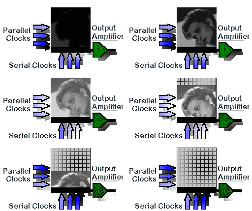

The Frame CCDs are devices in which the total area of
the CCD is available for sensing incoming photons during the exposure  period.
During readout of the CCD, charge is shifted sequentially across the array necessitating
the use of a shutter to prevent smearing for almost all exposure lengths. (Technically,if
the exposure time is much longer than the actual readout rate, then the level
of smearing can be quite small.) This format has 100% fill factor, which means
that 100% of each pixel area is being utilized to detect photons during the
exposure. The pixels are typically square in format so there is no image distortion
inherent to the detector. These devices are available with pixel sizes that
range from 6.8 microns square (Kodak 1400 CCD) up to 24 microns square (SITe
512 CCD) and with pixel formats of 512 × 512 up to 2k × 3k. The
full frame CCDs can come designed for front side illumination or for back side
illumination. With the front illuminated CCD, the light must traverse the SiO
2 gate structures overlying the photosensitive silicon called the depletion
layer. These gate structures are essential for pixel formation in the CCD, but
the differences in the indices of refraction between the gates and the silicon
causes shorter wavelength light to reflect off the surface of the CCD, reducing
the QE for those wavelengths.