
At higher wavelength (more than 600 nm) distance of charge generated
by photons in the silicon beneath the CCD electrodes ( pixel)
increases. At visible wavelength charge mostly generates in the
depletion region of the pixel. The electrical field in the depletion
region will force the charge to move to the nearest potential
well. At longer wavelength, charge will diffuse and not be collected
by the depletion region of a pixel, thus resulting in lower quantum
efficiency since charge generated at higher wavelength will not
be detected under the pixel. Specially in Raman spectroscopy a
high QE in the NIR is required and the new deep depletion CCDs
now available offer up to 35% QE at 1000 nm .
Deep Depletion CCD ( high resistivity
silicon substrate CCDs ).
This CCDs use a special high resistance silicon known as "epitaxial"
silicon. This material has a highly doped substrate that helps
to reduce the distance that charge generated by photons can diffuse
and would not be detected as a signal. Back illuminated deep depletion
CCDs can not be manufactured using MPP mode so they have a higher
dark current than our MPP mode CCDs . Even we offer thermo-electric
cooled deep depletion detectors, we do not recommended TE cooling.
This CCDs should only be ordered as liquid nitrogen cooled detectors.
Roper Scientific offers the 1340 EHRB NIR Optimized back-illuminated
and the 1340 EHR front illuminated CCDs fabricated in deep depletion
technology.
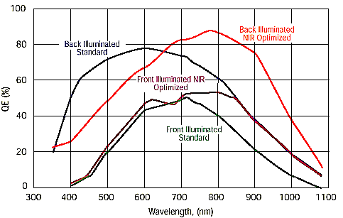
Chart: Comparison between conventional back-illuminated CCD
and PI's NIR optimized 1340 EHRB spectroscopy CCD
Advantages of deep depletion CCDs: