
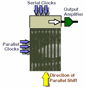
 The
interline CCD is a hybrid sensor with photosensitive diodes on
one part of the pixel which are electrically coupled to a CCD
type storage region which resides under a mask structure. The
masks are long structures running along the vertical axis of the
CCD alternating with the open regions, hence the name interline
CCD. The diode portion of the pixel has very good QE properties,
but the diode only takes up approximately 25% of the pixel area
(25 % fill factor), reducing the number of photons converted per
unit area.
The
interline CCD is a hybrid sensor with photosensitive diodes on
one part of the pixel which are electrically coupled to a CCD
type storage region which resides under a mask structure. The
masks are long structures running along the vertical axis of the
CCD alternating with the open regions, hence the name interline
CCD. The diode portion of the pixel has very good QE properties,
but the diode only takes up approximately 25% of the pixel area
(25 % fill factor), reducing the number of photons converted per
unit area.
Lens on Chip
As a way to drive up the fill factor, higher quality interline
CCDs have small lenses annealed to the CCD that bring the light
from a larger area down to the photodiode. This brings up the
fill factor to around 70% and results in a better net QE across
the visible spectrum than a CCD without the lenses. In this type
of CCD, the signal accumulates on the photodiode and is then rapidly
shifted to the adjacent CCD structure, taking approximately 1
microsecond to perform the transfer. This extremely fast transfer
means that the smearing will be non-detectable for any exposure
of a millisecond or longer. In addition, this type of rapid shifting
allows for some interesting uses of the interline CCD such as
very short exposures for fast moving objects and is an ideal CCD
to use with “slow gating” types of measurements.
Exview HAD,
a new Technology Improves Overal Quantum Efficiency of Interline
CCDs
Sony improved the microlens technology with the introduction of Super HAD CCD
(HAD, stands for Hole Accumulation Diode). Super HAD CCDs
have much closer spacing between microlenses, thus further increasing the light
collection efficiency.The latest of Sony's innovations is introduction of additional
layer of on-chip microlens very close to the pixel area. When used with wider
f-stops, single array of microlens can not focus the parallel beams on to the
sensing area of the pixel, reducing the sensitivity. Second layer of lenses
helps alleviate this problem by further condensing the beam path, consequently
increasing QE. Another improvement in this technology is thinning of insulating
layer between Si substrate and poly Si gate structures, reducing the smear factor
(light leaking under the mask). With the introduction of EXview HAD CCDs, Sony
took the interline technology another step by improving the QE in near infrared
(NIR) region. As the NIR photons are absorbed in deeper part of the Si, using
thicker Si, increases the probability of photon-Si interaction and thus QE.
Our new CoolSNAP HQ uses the EXview HAD technology
Roper Scientific has engineered the read out of the Exview HAD CCDs to bring the full well to the absolute
highest level while maintaining linearity throughout the imaging
range of the device. Getting the readout noise even at 20 MHz
to the lowest level possible allows the maximum in dynamic range
performance.
Note:
Quantum efficiency (QE) is the probability of a photon being absorbed
in the Si. By allowing the more light reach the Si, QE is increased.
Quantum efficiency, often expressed as a percentage, indicates
the effectiveness of an imager to produce electronic charge from
incident photons. The greater the QE at a given wavelength, the
more efficient the imager at that wavelength.