
Roper Scientific's Virtual Chip Mode
A novel CCD readout technique that delivers 16 bit images at frame
rates in excess of 600 fps.
Introduction
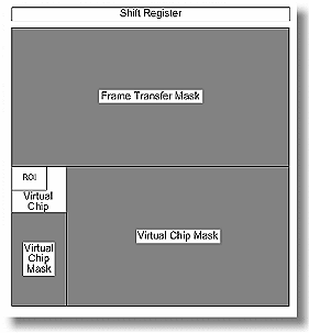
In operation, images are continually piped down the CCD at extraordinarily
high frames per second (FPS). The mini-frame transfer region is
defined by an ROI as illustrated in Figure 1. The charge from
this ROI is shifted under the frame-transfer mask, followed by
a readout cycle of an ROI-sized region under the mask. Since the
ROI is far from the serial register, the stored image is just
shifted repeatedly with the readout and the first few images collected
will not contain useful data. After the readout period, the next
frame is shifted under the mask and another ROI sized frame is
read out. The net result is a series of images, separated by spacer
regions, streaming up the CCD under the mask. Refer to Table 1
for a listing of virtual chip sizes with their respective readout
times and frame rates per second. Masking can be achieved by applying
a mechanical or optical mask or by positioning a bright image
at the ROI against a dark background on the remainder of the array.
The online timing calculator reports the readout time that will
result with the current virtual-chip parameter values like subarray
x and y dimension, the binning values, the exposure time and the
shutter compensation time.
| ROI (NxN) | 1MHz (msec) | 1MHz (FPS) | 100kHz (msec) | 100kHz (FPS) |
| 164 | 29.8 | 33.6 | 287 | 3.5 |
| 96 | 10.9 | 91.7 | 102 | 9.8 |
| 84 | 8.65 | 115 | 79.8 | 12.5 |
| 64 | 5.26 | 190 | 47.6 | 21.0 |
| 56 | 4.22 | 237 | 37.4 | 36.7 |
| 47 | 3.08 | 324 | 26.9 | 37.2 |
| 36 | 1.97 | 507 | 16.6 | 60.2 |
| 30 | 1.51 | 662 | 12.2 | 82.0 |
 |
System requirements for the Virtual Chip option :
Tips on masking
the CCD
If mechanical masking is used, the mask can be a static one (fixed
dimensions) in which case, multiple masks should be made to accommodate
a variety of imaging conditions. Alternatively, a more flexible
mask can be manufactured by taking two thin metal sheets with
a square hole the size of the exposed region of the CCD cut in
the center. This would be 512 × 512 pixels at 13 microns
per pixel = 6.7 mm × 6.7 mm for the MicroMAX 512 BFT. These
masks should be anodized black to prevent reflections in the optical
system and they should be very flat. These two sheets can then
be slid relative to one another to achieve any rectangular shape
required. The sheets should be placed flat in the optical plane
and their openings should be centered on the optical axis. Ideally
they should be able to move with an accuracy of 2-3 pixels per
step (30-45) in the X and Y directions.